The Semiconductor Industry's SiC Dilemma: Material Challenges vs. Manufacturing Reality
 June 13, 2025 5:19 pm
The semiconductor industry is at an inflection point. As new energy vehicles (NEVs), 5G, and AI drive demand for higher-power, high-frequency devices, silicon carbide (SiC) has emerged as the material of choice. Compared to traditional silicon, SiC offers: 10x higher breakdown electric field strength, 3x higher thermal conductivity, and 50% lower energy losses in power electronics.
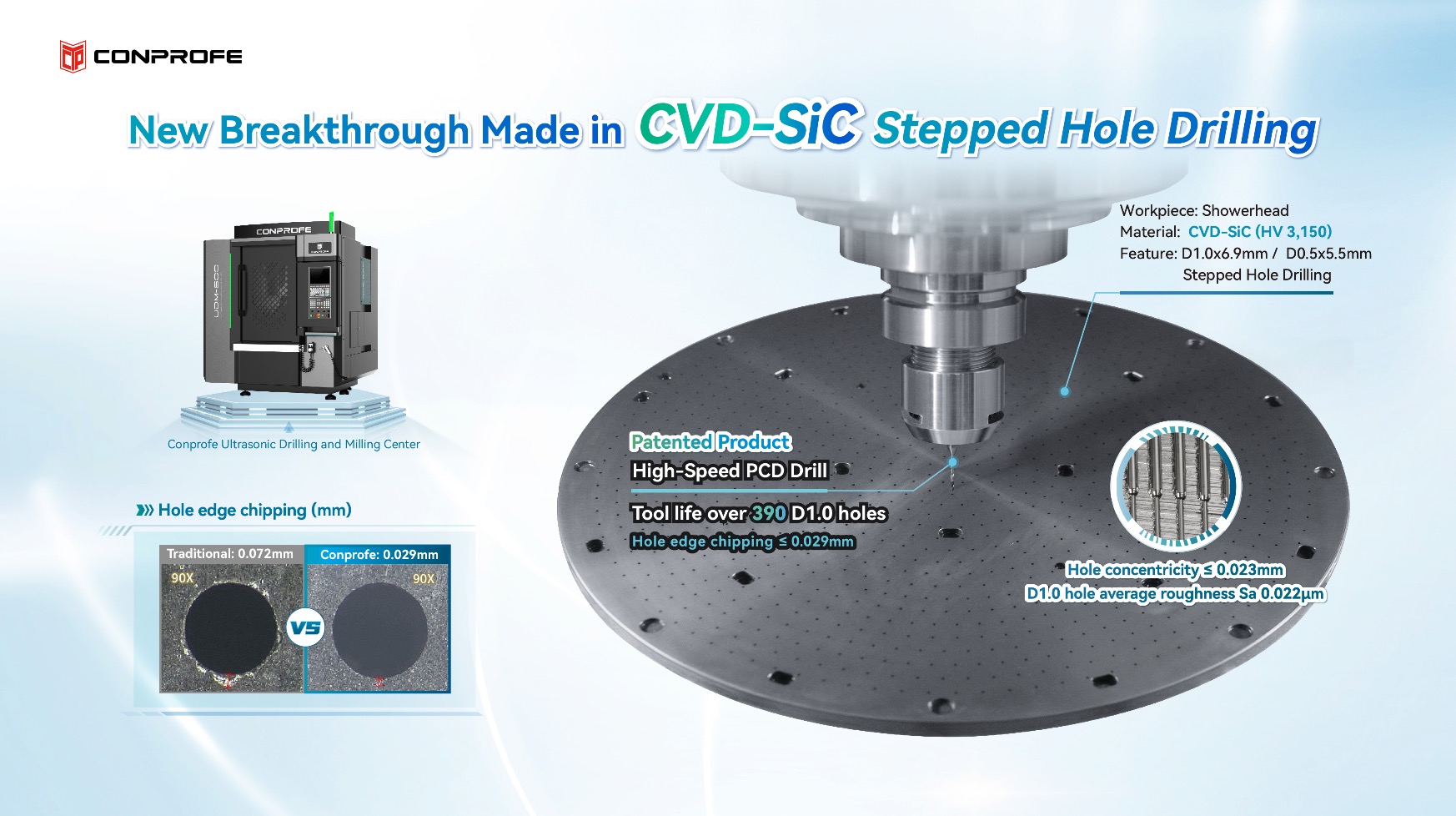
Major players like Tesla, Infineon, and STMicroelectronics are rapidly adopting SiC for MOSFETs, diodes, and substrates. However, this transition hinges on one critical bottleneck: manufacturing scalability. With SiC wafer production growing at 30% CAGR (Yole Développement, 2023), the ability to machine complex components—like showerheads for wafer etching and cleaning equipment—with micron-level precision, will determine who leads the next semiconductor decade.
Material-Specific Challenges: The Hard Truth About SiC
Extreme Hardness & Brittleness: Mohs 9.5 hardness (vs. silicon’s 6.5) accelerates tool wear by 20–50x; low fracture toughness causes micro-cracks under mechanical stress, compromising device reliability
Anisotropic Crystal Structure: Directional hardness variations lead to inconsistent cutting forces; cleavage planes promote uncontrolled crack propagation during drilling
Thermal Sensitivity: High thermal conductivity (120 W/m·K) rapidly transfers heat to tools; thermal shock risk at >800°C induces subsurface damage
Process Pitfalls: Where Traditional Methods Fail
Tool Degradation: Diamond tools last <15 holes in conventional drilling before edge rounding; cost per hole spikes due to frequent tool changes
Geometric Defects: Tapered holes (>0.05mm deviation) from tool deflection; edge chipping (>50µm) ruins wafer uniformity in CVD applications
Heat Management: Coolant contamination risk in semiconductor-grade components; thermal stress alters SiC’s electrical properties
Surface Integrity: Subsurface cracks (5–10µm deep) act as failure initiation sites; Ra > 0.5µm necessitates costly post-polishing
Conprofe’s Ultrasonic Solution: A Paradigm Shift
Ultrasonic-Assisted Machining (UAM): 15-70kHz vibrations significantly reduce cutting forces, extending tool life to 100+ holes; crack suppression via controlled micro-fracture mechanics
Process Innovations: Diamond-coated tools with optimized flute geometry for chip evacuation; cryogenic air blasting options for heat-sensitive applications
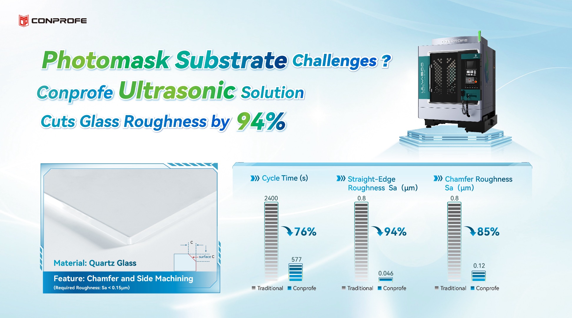
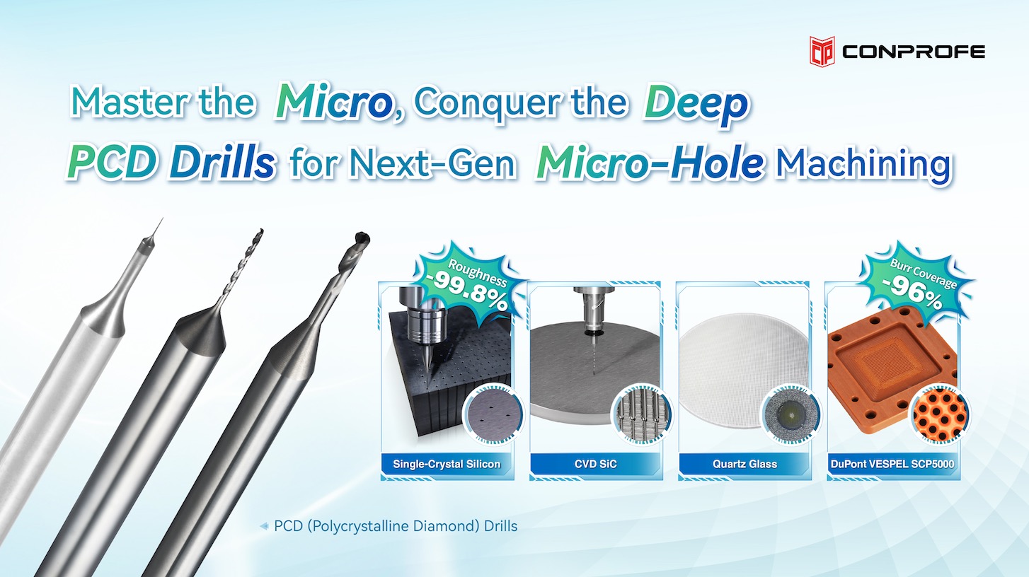
Quantifiable Results for SiC Showerhead Case: Continuous and stable drilling of over 100 holes (vs. industry avg. of 15-20 holes); smooth hole wall and good hole quality (hole chipping size <0.02mm)
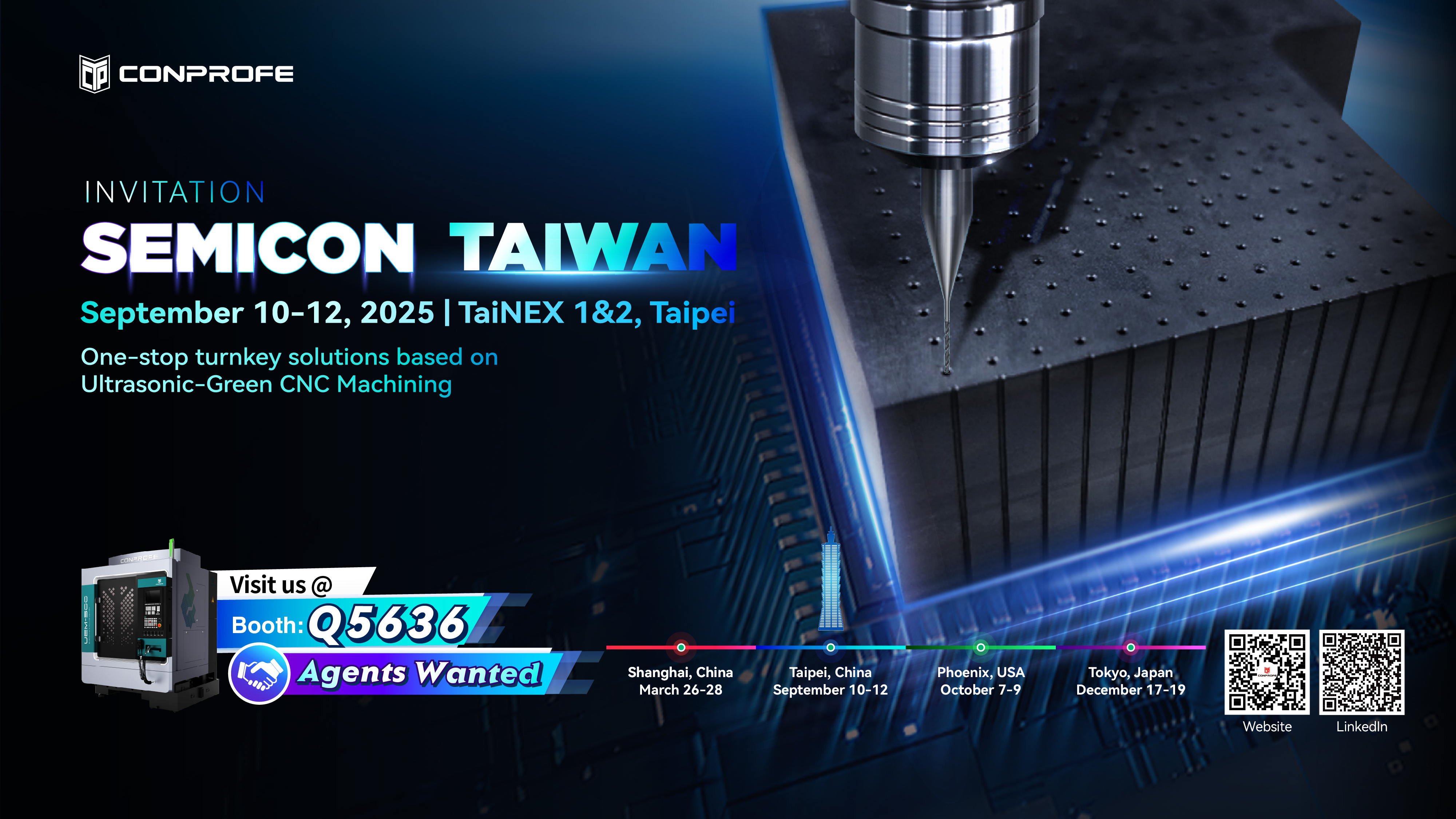
Where to See Us Next
Join Conprofe at these pivotal 2025 events in semiconductor industry to discuss SiC’s future:
· SEMICON Taiwan (Sep. 4-6, Taipei)
· SEMICON West (Nov. 12-14, Phoenix)
· SEMICON Japan (Dec. 11-13, Tokyo)
Stay tuned for upcoming Application Cases and our Ultrasonic Machining Solutions to solve your challenges!