Solving the Engineering Plastic Challenge: Conprofe Solution Enables 0.2% Micro-Hole Defect Rate in Test Socket
 July 8, 2026 4:40 pm
In the high-stakes world of semiconductor manufacturing, yield is paramount. The final test phase, where chips are validated for performance and functionality, relies heavily on a critical yet often overlooked consumable: the semiconductor test socket. This hardware, typically composed of probes, electronic components, and a printed circuit board (PCB), forms the vital electrical bridge between the wafer and the test system. Its precision directly impacts chip yield, test cost, and overall manufacturing efficiency. As chip architectures continue to shrink and become more complex, the demand for higher precision and quality in these test sockets has never been greater.
The Manufacturing Challenge
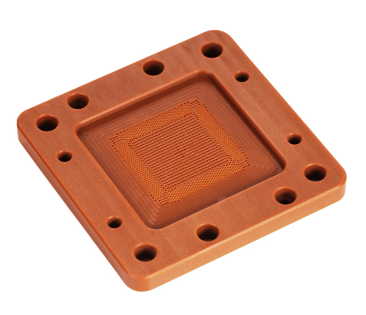
Engineering plastics, known for their exceptional insulation, heat resistance, and chemical stability, are the material of choice for manufacturing these high-precision sockets. However, machining these materials, particularly for applications requiring dense arrays of stepped micro-holes, presents a formidable engineering challenge. Conventional machining methods often struggle to balance high accuracy with production efficiency.
The primary issues stem from the inherent properties of the material and the demanding geometries:
Machining Instability: Creating intricate, dense hole patterns with tight tolerances on a highly-customized part demands extreme stability, which is difficult to achieve with traditional processes.
Burr Formation: The ductile nature of engineering plastics means high-speed drilling often generates significant exit burrs. These burrs are more than just a cosmetic flaw; they can interfere with probe contact, leading to test inaccuracies and potential chip damage. Removing them adds a costly secondary operation and risks scrapping the part.
The Conprofe Solution: An Integrated Ultrasonic Approach
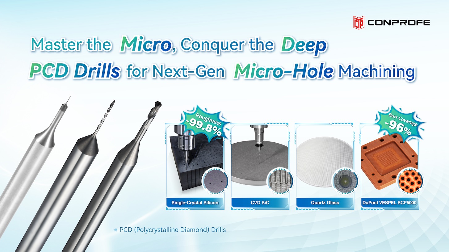
Conprofe, a leader in advanced Ultrasonic-Green CNC Machine Tools, has successfully tackled these challenges with an integrated solution. Recently, a customer facing critical bottlenecks in machining stepped micro-holes in DuPont’s Vespel SCP5000 engineering plastic achieved remarkable results using Conprofe’s proprietary technology stack.
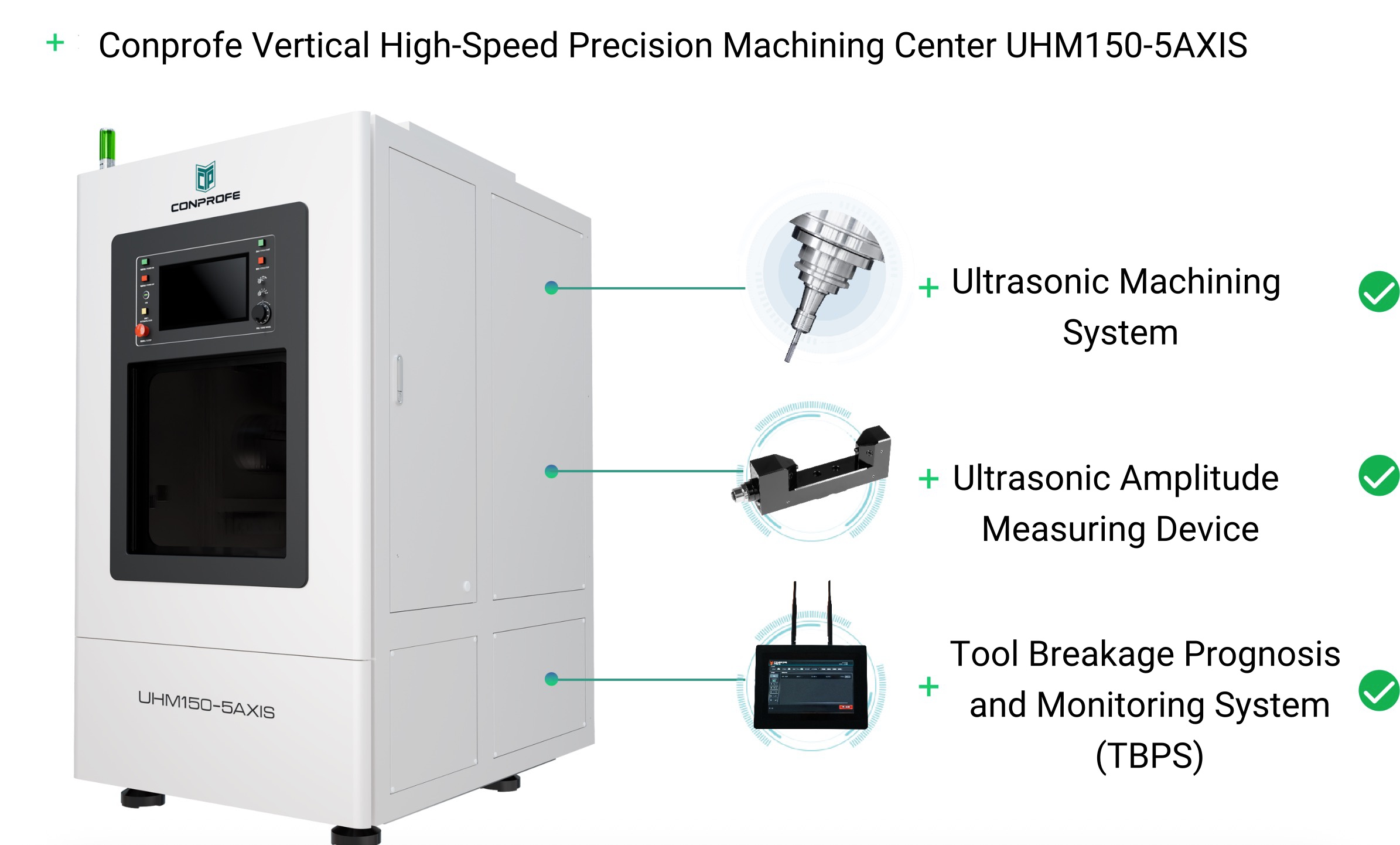
Our solution, centered around the Conprofe Vertical High-Speed Precision Machining Center UHM150-5AXIS, incorporates several key technologies:
Intelligent Ultrasonic Machining: This core technology reduces cutting force, improves chip evacuation, and minimizes tool wear, enabling stable, high-quality machining.
Ultrasonic Amplitude Measuring Device: This ensures the ultrasonic system is operating at peak performance for consistent and repeatable results.
Tool Breakage Prognosis and Monitoring System (TBPS): This advanced monitoring system prevents catastrophic tool failure, ensuring uninterrupted, automated production and protecting the workpiece.
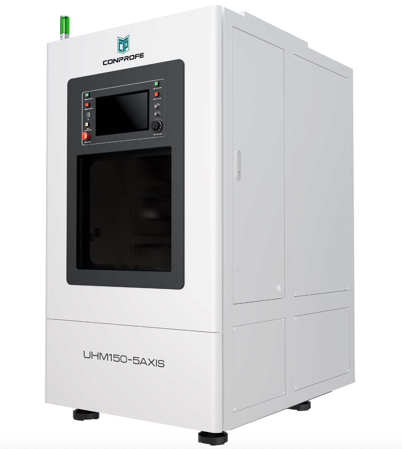
Conprofe Vertical High-Speed Precision Machining Center UHM150-5AXIS features a compact design and small footprints, with a total weight of only 1,500kg. It is equipped with Conprofe’s proprietary Intelligent Ultrasonic Machining System and offers the option of a 40,000rpm ultrasonic spindle or a 160,000rpm high-speed air-bearing spindle. The machine tool is paired with a proprietary high-rigidity, high-precision rotary table, with B/C-axis positioning accuracy of ±5 arcsec and repeatability of ±2 arcsec. It is equipped with high-precision linear encoders, achieving X/Y/Z-axis positioning accuracy of 2μm and repeatability of 1μm. The machine also features a horizontal-carousel-type tool magazine (24T) and is suitable for high-speed milling and drilling applications across a wide range of high-precision products in the semiconductor industry.
Key Results: Setting a New Benchmark in Micro-Hole Quality
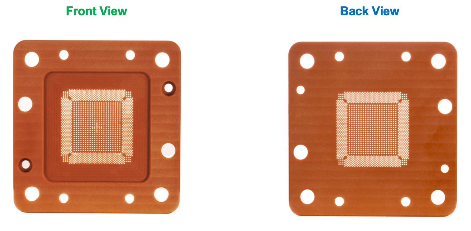
The results of implementing the Conprofe solution on stepped micro-holes (D0.2/D0.3mm) were transformative. The solution not only met but significantly exceeded the customer’s stringent quality requirements.
Stepped Micro-Hole Machining of Semiconductor Test Socket
Material: DuPont engineering plastic (VESPEL SCP5000)
Feature: Stepped micro-hole drilling, D0.2/D0.3mm
Inspection Equipment and Method
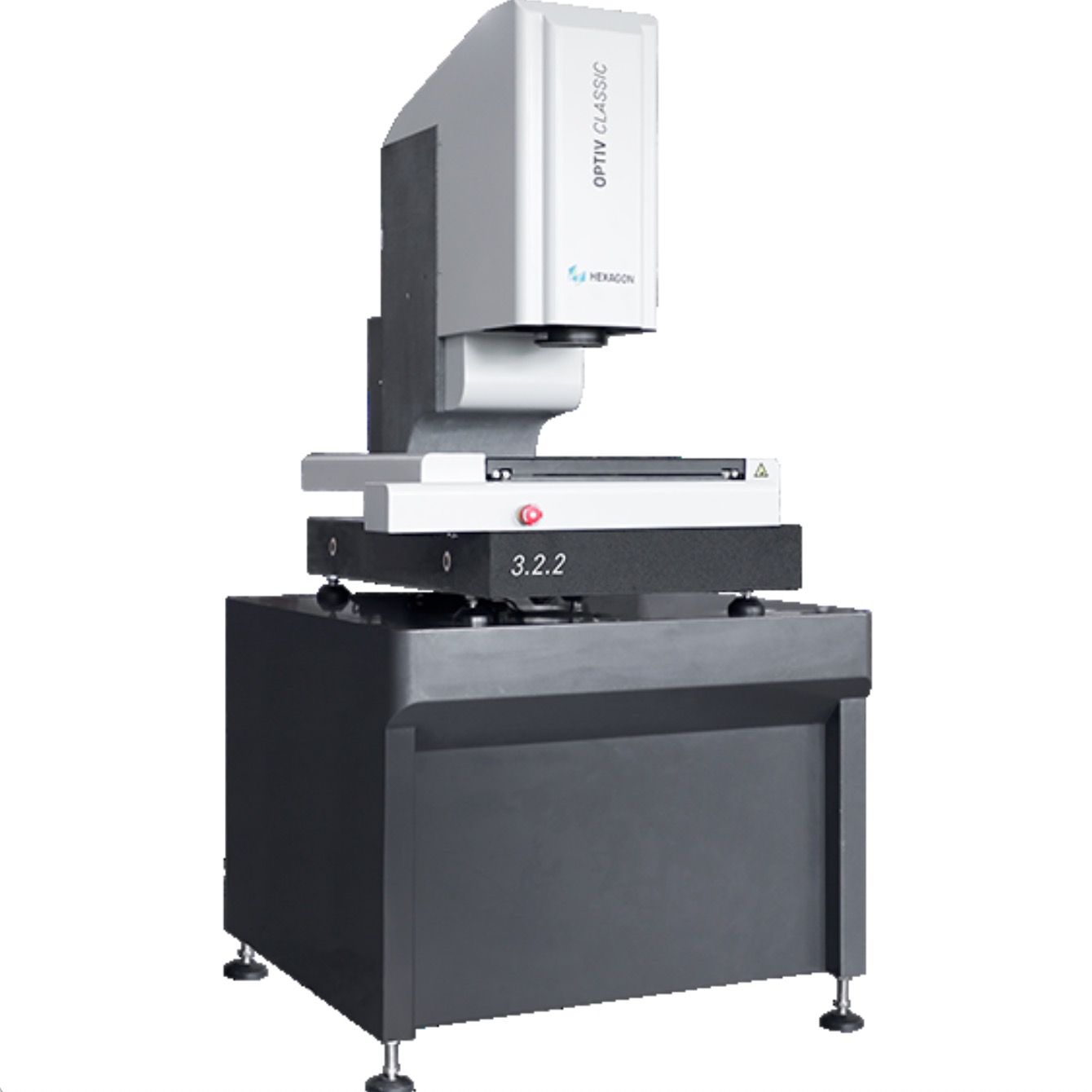
Inspection Equipment: HEXAGON OPTIV CLASSIC VMM
Inspection Method: Dimensional and surface quality inspection of workpieces
The Conprofe solution delivered exceptional burr suppression performance. Quality inspections across 168 sets of holes verified that all critical dimensional and geometric tolerances—including diameter, roundness, positional accuracy, and coaxiality—were consistently met. In addition, all 15 sets of chamfers inspected fell well within the required depth tolerances, and every positioning hole angle complied with specifications.
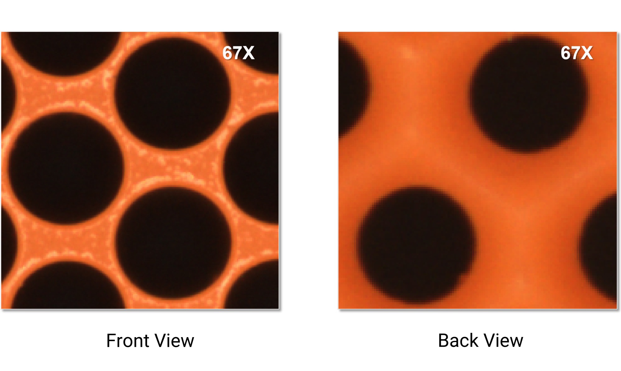
Superior Hole Wall Integrity: The process maintained a minimum hole pitch of just 0.35mm and a minimal wall thickness of 0.03mm, with exceptional consistency and no instances of wall breakage.
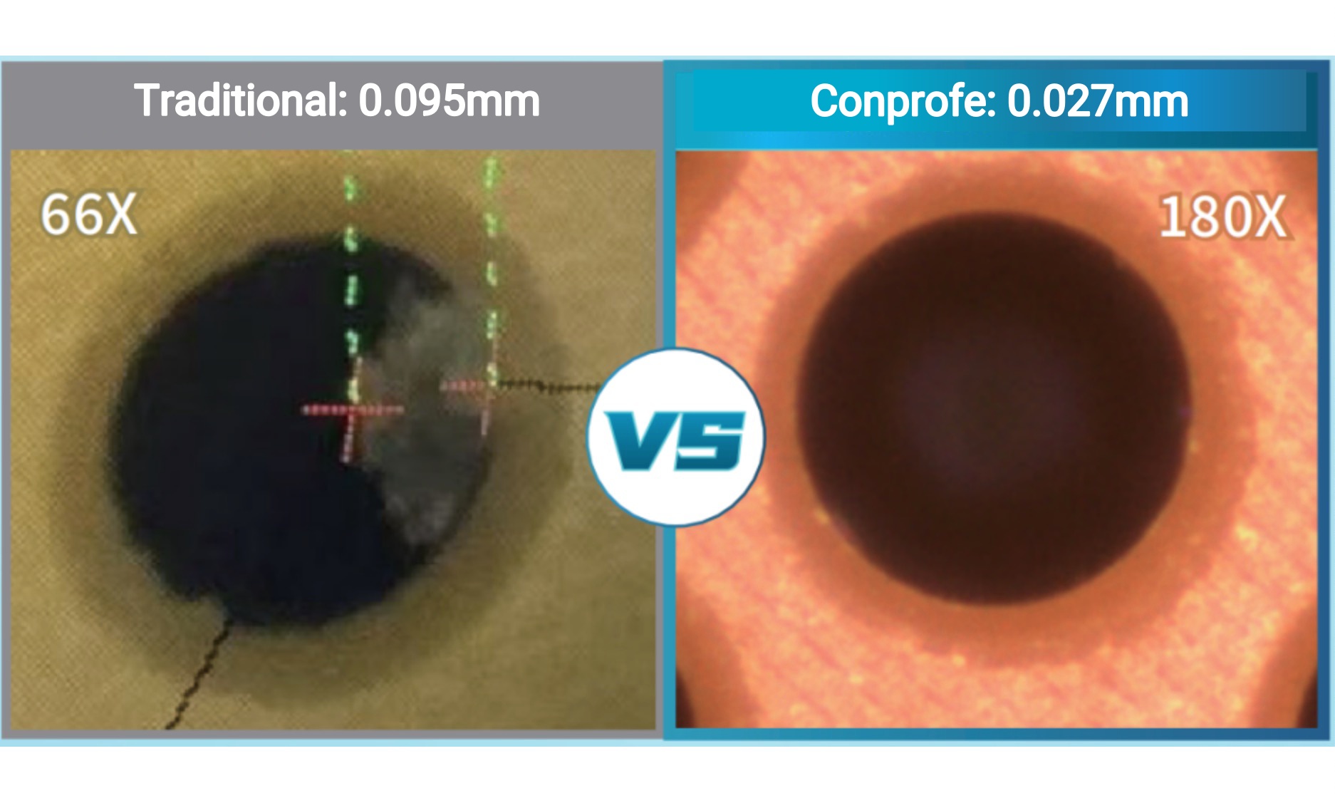
Dramatic Reduction in Burrs: The average entrance/exit burr height was reduced from 0.095mm to just 0.027mm—a 72% improvement. This drastically cuts or even eliminates the need for a secondary deburring step.
Unprecedented Yield Improvement: The most striking metric is the defect rate for micro-hole burrs. While conventional methods struggle with a 5% defect rate, the Conprofe solution achieved a staggeringly low defect rate of just 0.2%. This means 99.8% of all micro-holes met quality standards, directly translating to significantly higher yields and lower production costs.
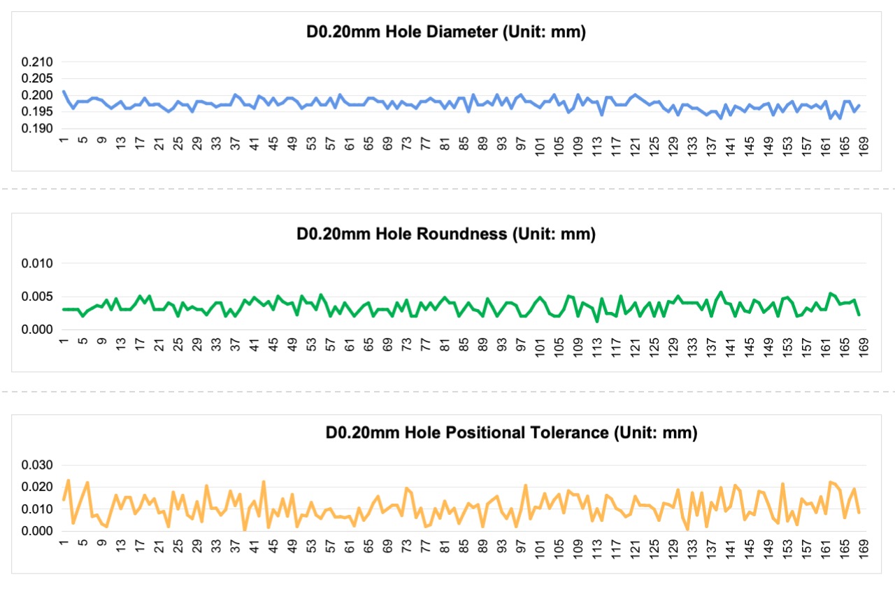
D0.2 Hole Geometric Tolerances: Diameter Range: D0.193mm-D0.201mm (Target: D0.20±0.01mm); Roundness: 0.001mm-0.006mm (Target:≤0.01mm); Positional Accuracy: 0.000mm-0.023mm (Target: ≤0.03mm)
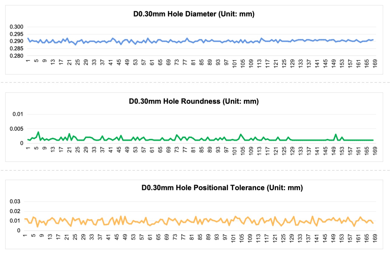
D0.3 Hole Geometric Tolerances: Diameter Range: D0.288mm-D0.292mm (Target: D0.30+0/-0.02mm); Roundness: 0.001mm-0.004mm (Target: ≤0.01mm); Positional Accuracy: 0.004mm-0.015mm (Target: ≤0.03mm)
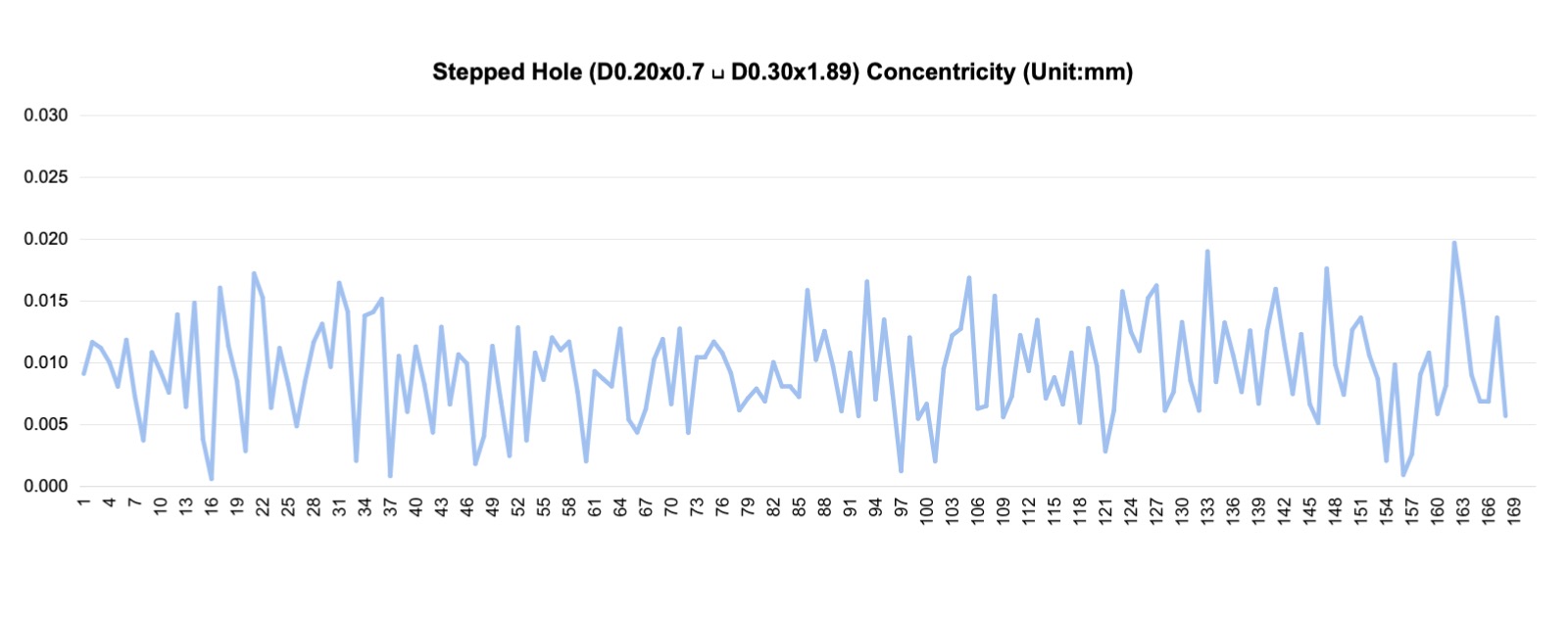
Hole Coaxiality: Customer target value ≤0.03mm; Conprofe ultrasonic solution achieved a coaxiality range of 0.001mm-0.020mm.
Chamfer Depth: 0.16mm+0.07/0mm (Target: +0.07/0mm)
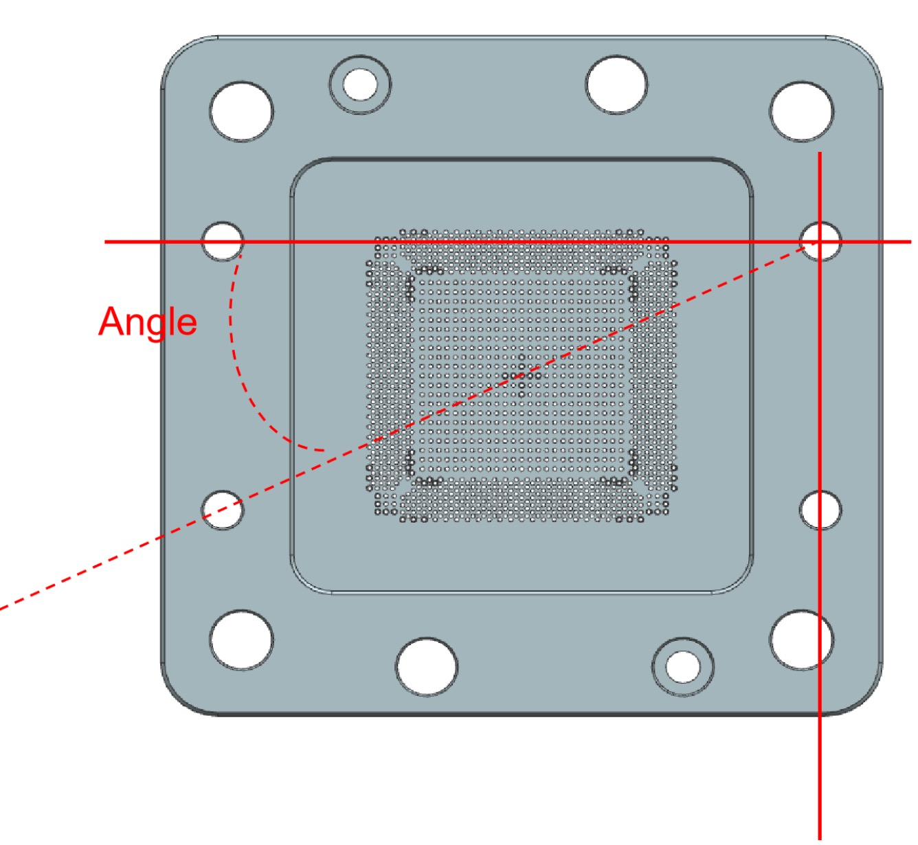
ATAN: Met standard value. Based on CMM measurement results, the angle shown in the above diagram is ATAN (15.000/31.501) = 25.463 (standard value: 25.463).
Beyond Test Sockets: Broad Applicability in Semiconductor Manufacturing
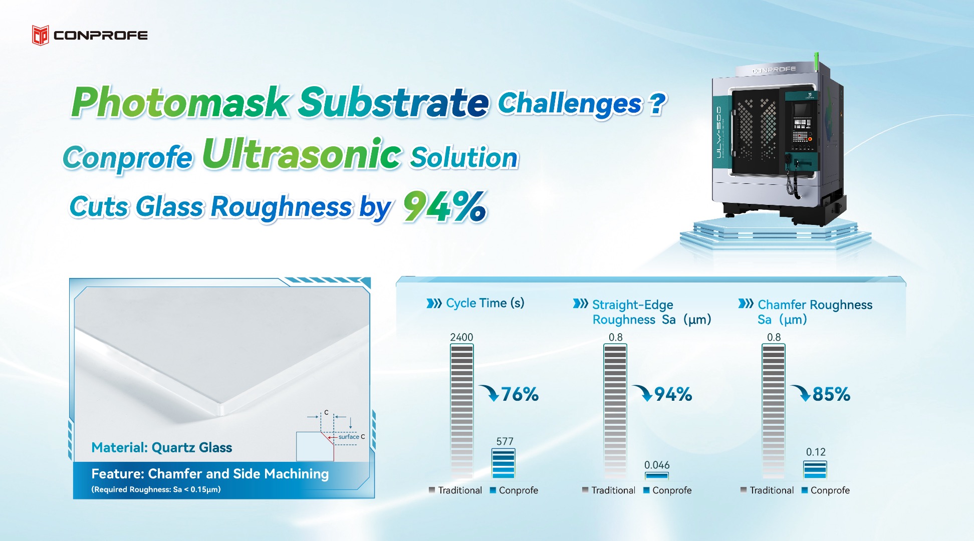
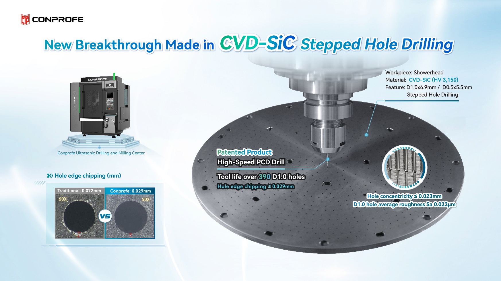
While this case study highlights a significant victory for test socket production, the underlying technology is applicable across a wide range of advanced materials and precision components in the semiconductor industry. Conprofe’s ultrasonic solutions have also proven highly effective in machining: CVD Silicon Carbide (SiC) showerheads, single-crystal silicon curved electrodes, quartz glass showerheads and substrates, alumina ceramic and aluminum alloy showerheads, high-temperature rubber probe nozzles, and AlSiC workpieces.
The Path Forward
As China’s semiconductor industry expands, the reliance on imported consumables like high-end test sockets remains a strategic concern. Conprofe is committed to providing the advanced, proven manufacturing solutions that enable the industry to move towards greater self-reliance and technological excellence. By combining deep expertise in material science with precision machine tool design and intelligent processing technologies, we are helping our partners overcome their most difficult machining challenges, improve efficiency, and elevate the quality of their final products.